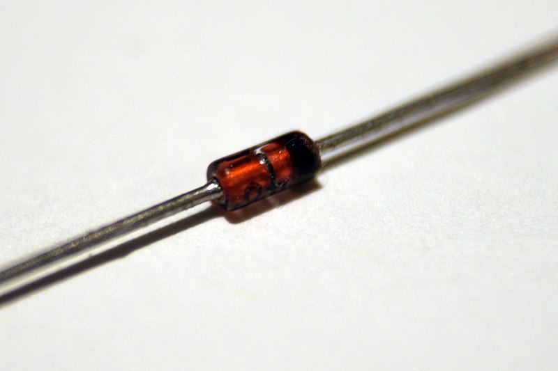
Zener diode characteristics and applications

Zener diode characteristics and applications

Zener diode is a reverse-biased heavily doped silicon diode named after the invention by C.Zener. Zener diode is specially designed to operate in the breakdown region. The doping level of silicon diodes can be varied as per breakdown voltages needed from 2V to 1000 V.

 The maximum reverse bias applied before entering into the Zener region is called the Peak Inverse Voltage. It is commercially referred to as PIV rating.

zener diode symbol
Zener diode symbol By ZyMOS – Own work, Public Domain, https://commons.wikimedia.org/w/index.php?curid=5617769

Application of Zener Diode in daily life

  • Voltage regulator
  • Peak Clippers
  • Calibrating voltages

Author: Pravin Babu R

I've done a Master of Engineering in Computer Science and B.Tech in Information Technology . Worked in a private IT company for 5 years. Currently preparing for the Civil Services Exam. My hobby is blogging in different Niches, especially technologies.

* * All the Notes in this blog, are referred from Tamil Nadu State Board Books and Samacheer Kalvi Books. Kindly check with the original Tamil Nadu state board books and Ncert Books.